
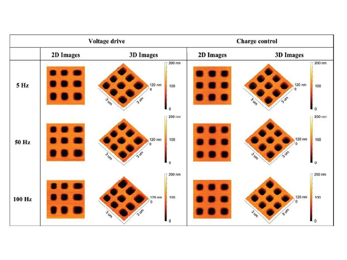
Precision Mechatronics: Atomic Force Microscopy (AFM)

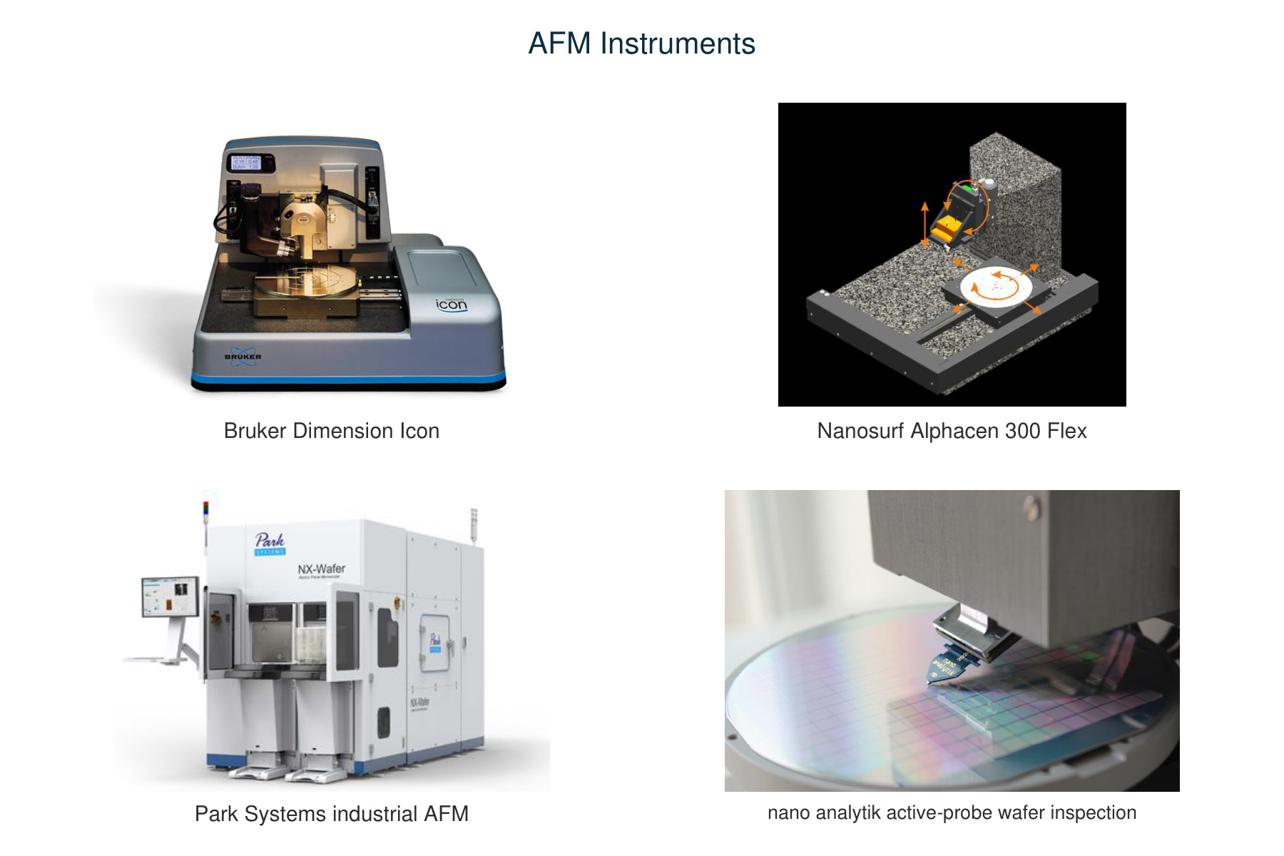
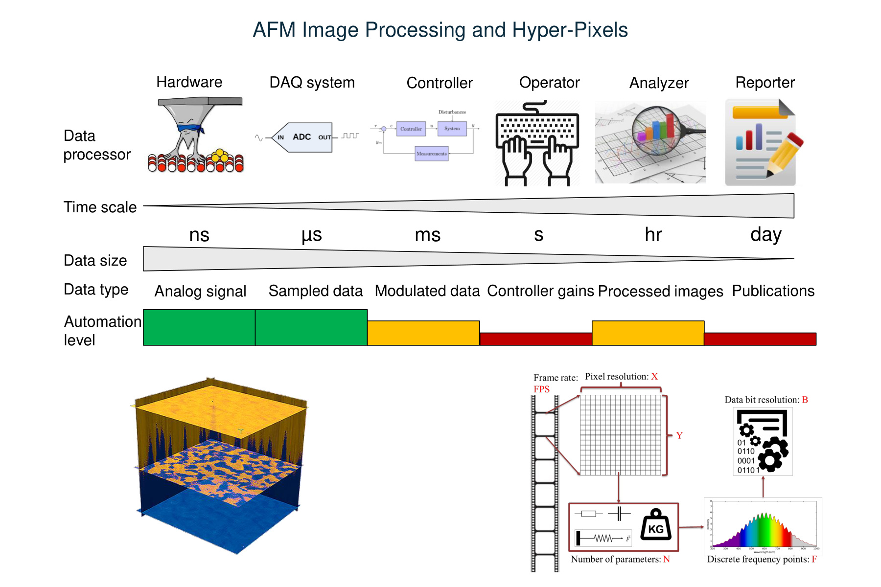
We develop atomic force microscopes that measure more surface area, capture faster nanoscale dynamics, and access features that conventional probes cannot easily reach. Our goal is high-throughput imaging that preserves the precision and sensitivity needed for semiconductor inspection and fundamental materials research.

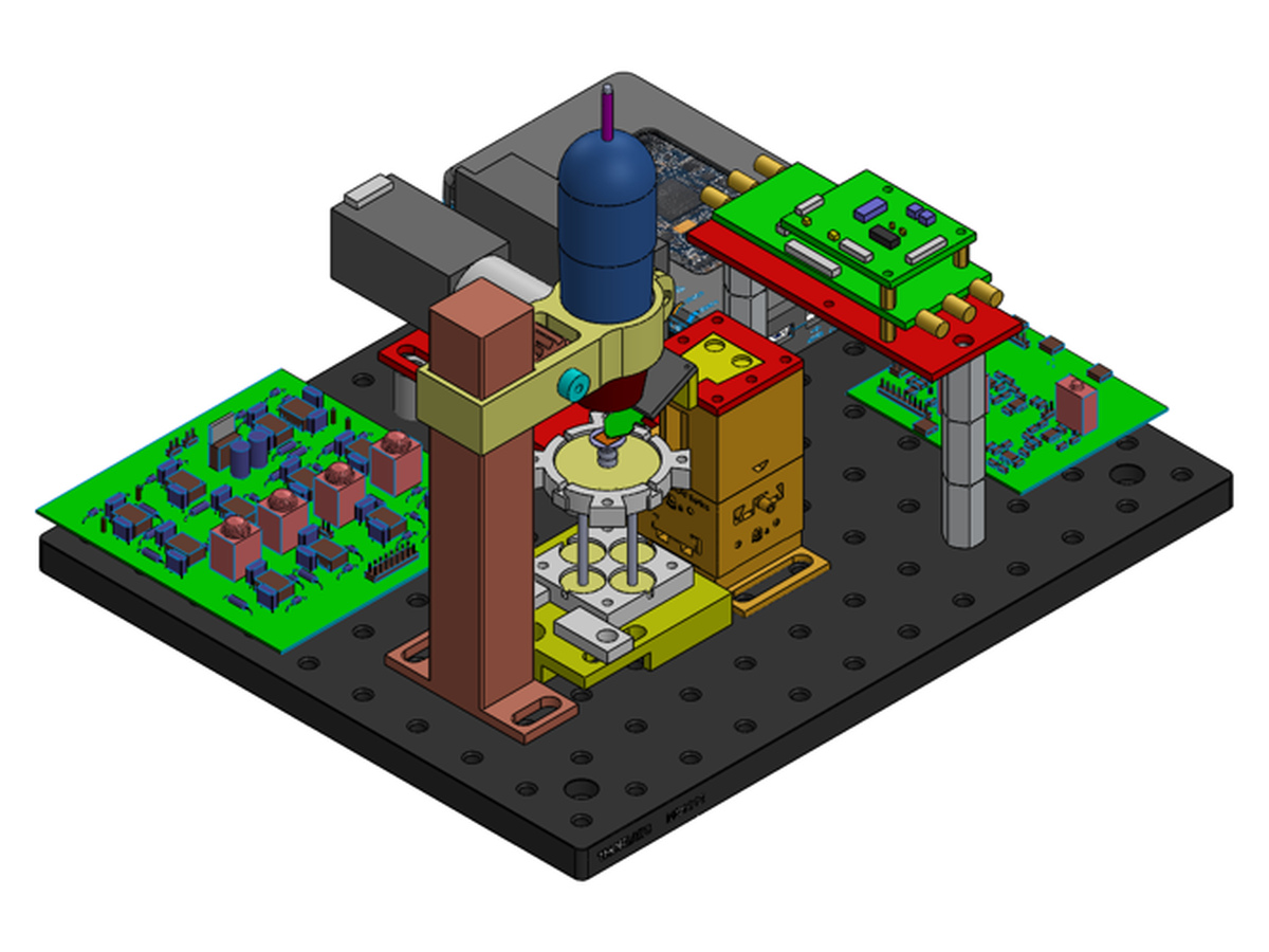
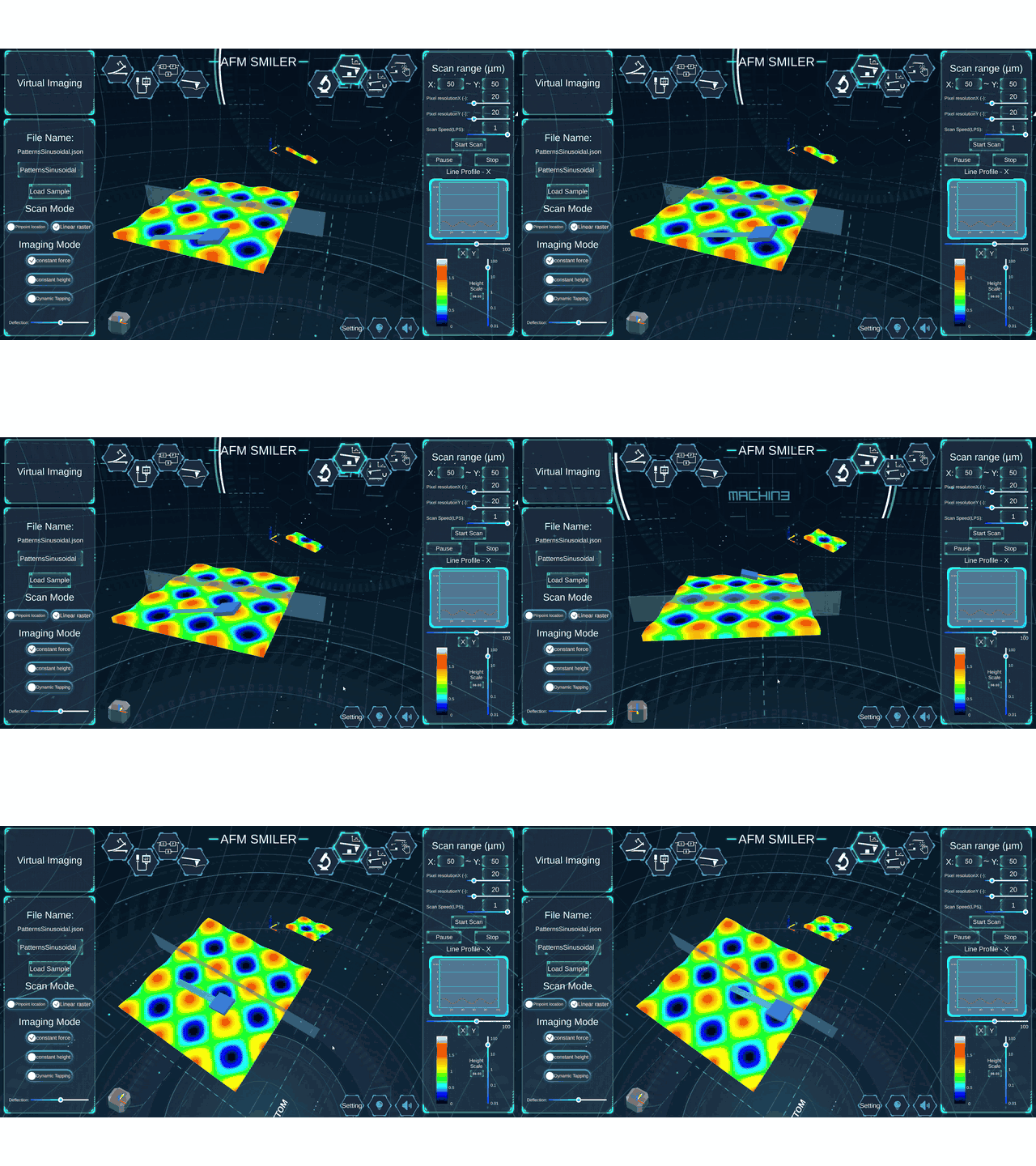
Our work connects active cantilever design and nanofabrication with large-range nanopositioning, fast imaging, multi-probe alignment, and feedback control. Current efforts include wafer-scale inspection, specialized probes for complex geometries, thermal-actuator compensation, and instruments for cryogenic and quantum-material studies. Hands-on AFM platforms and interactive simulations bring these ideas into mechatronics education.

Research Image Gallery

Special-Feature Imaging

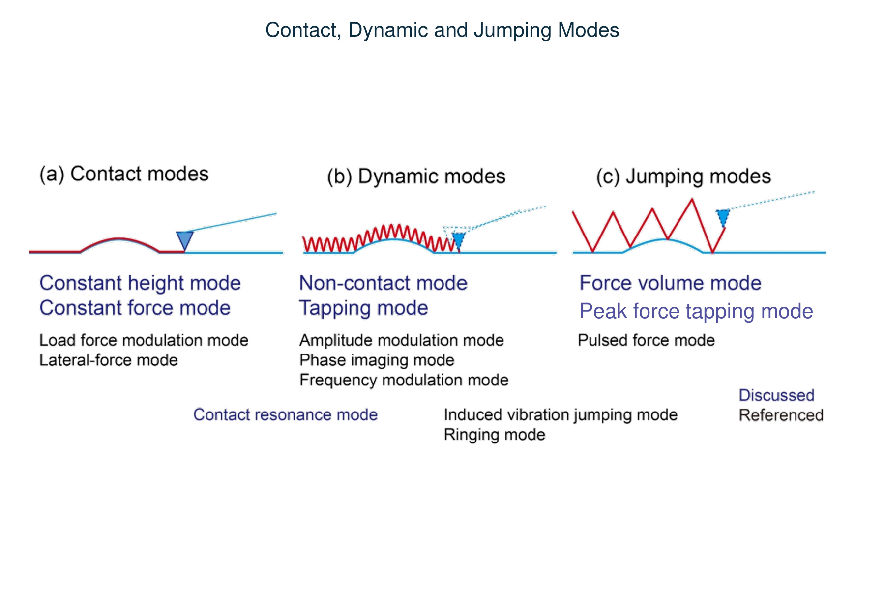
We develop specialized AFM probes and sensing methods for complex features and material properties.

  • Objective: Develop measurement capabilities for high-aspect-ratio features and subsurface electrical contrast.
  • Significance: Access geometric and electrical information beyond conventional topographic imaging.
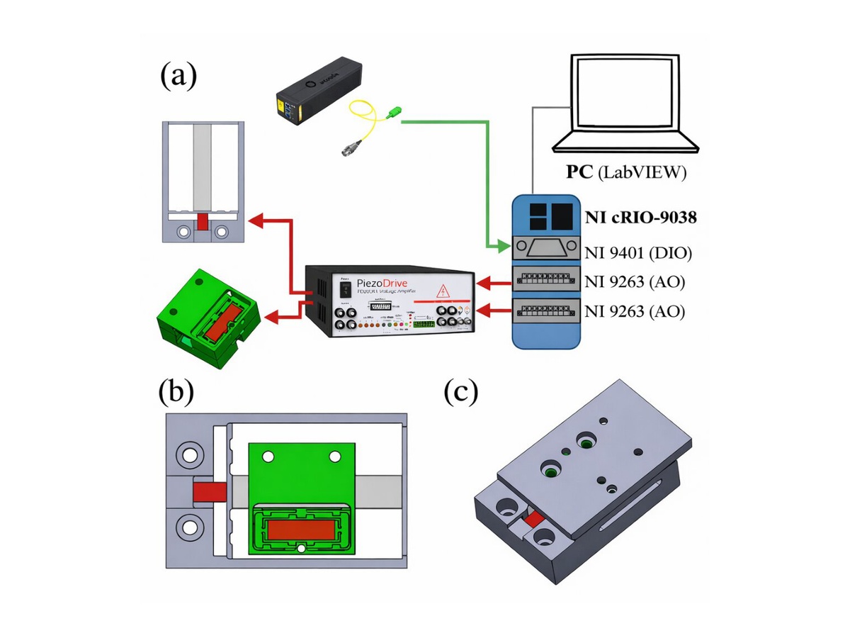
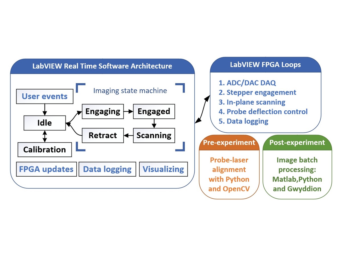
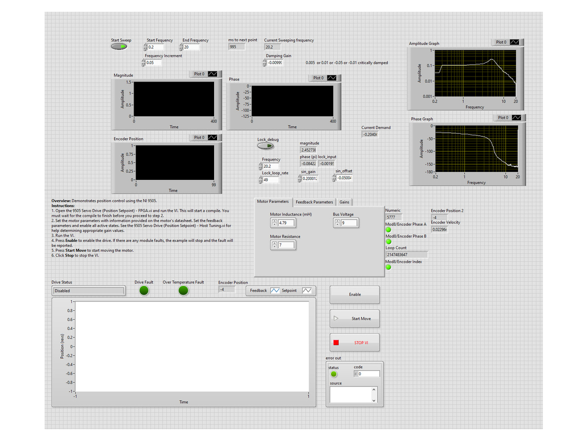
  • Result: Established a Nanosurf DriveAFM platform with LabVIEW control and specialized probe capabilities. Scanning microwave microscopy electronics and hardware integration are in development.
Nanosurf DriveAFM platform for specialized-geometry imaging.

Nanosurf DriveAFM Platform

Nanosurf DriveAFM platform for specialized-geometry imaging.

High-aspect-ratio electron-beam-deposited AFM tip, shown in a reference product image.

High-Aspect-Ratio Reference Tip

High-aspect-ratio electron-beam-deposited AFM tip (reference product image).

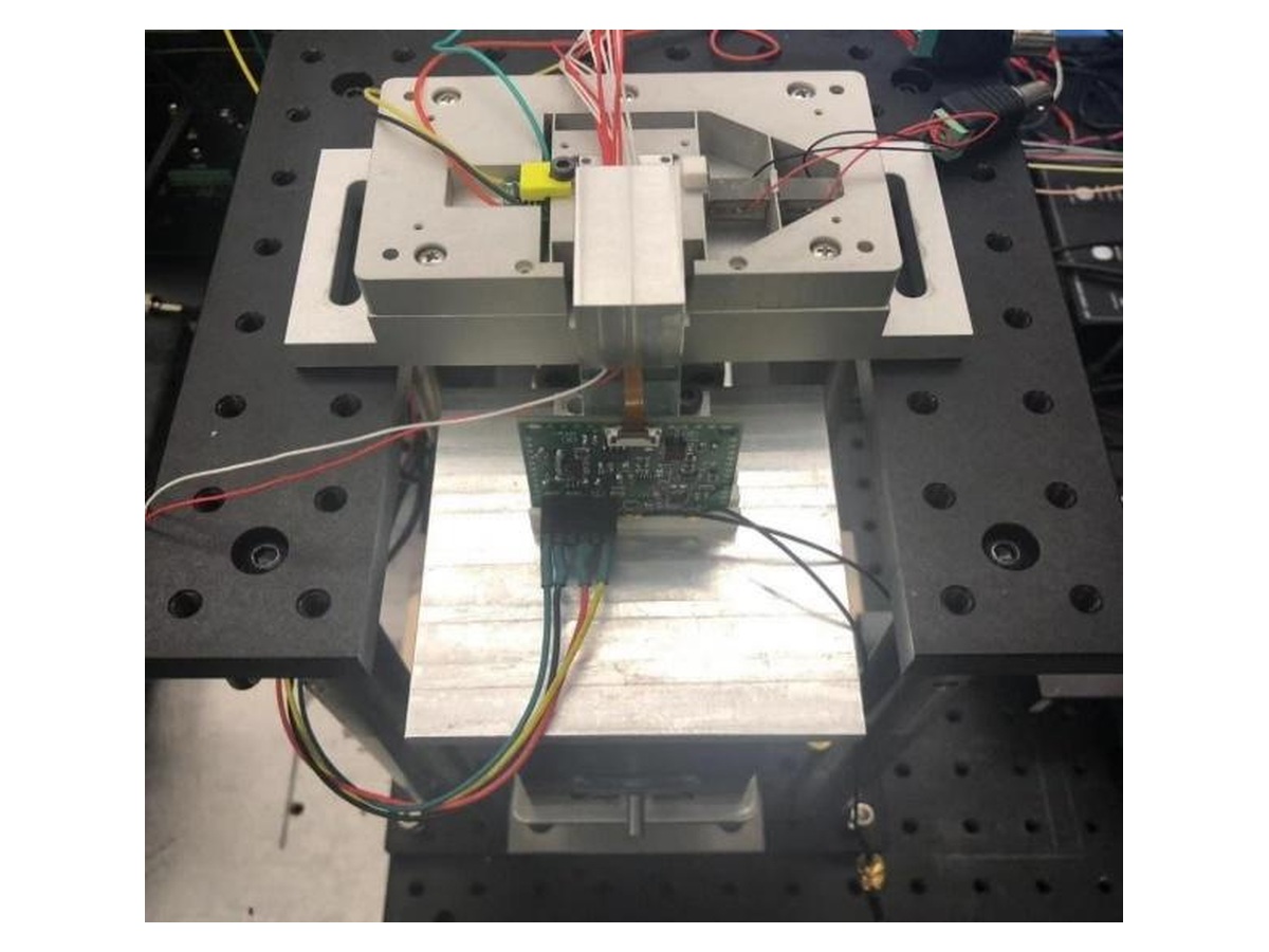
Electronics and custom PCB assembled for the scanning microwave microscopy project.

Microwave Readout Electronics

Electronics and custom PCB assembled for the scanning microwave microscopy project.

Active-Probe Wafer Inspection

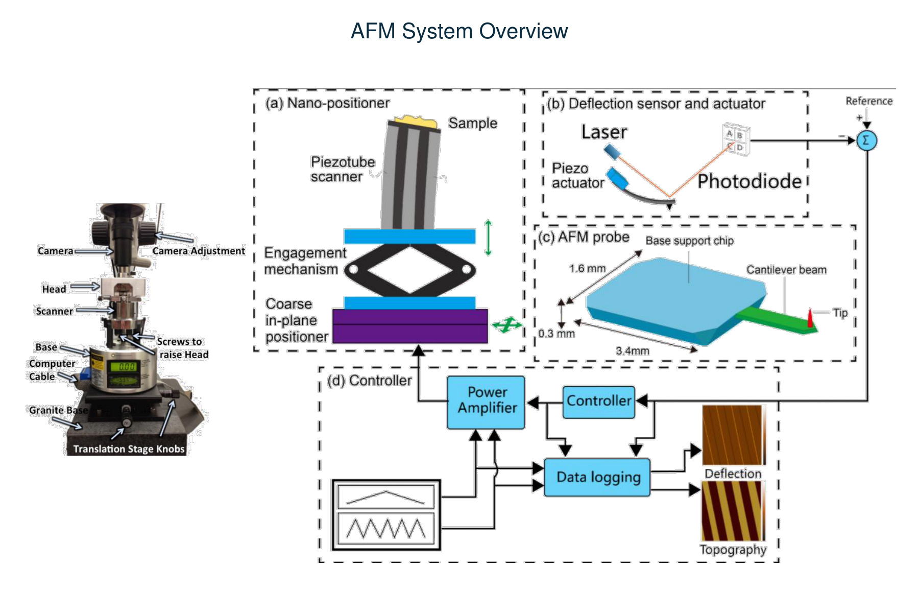
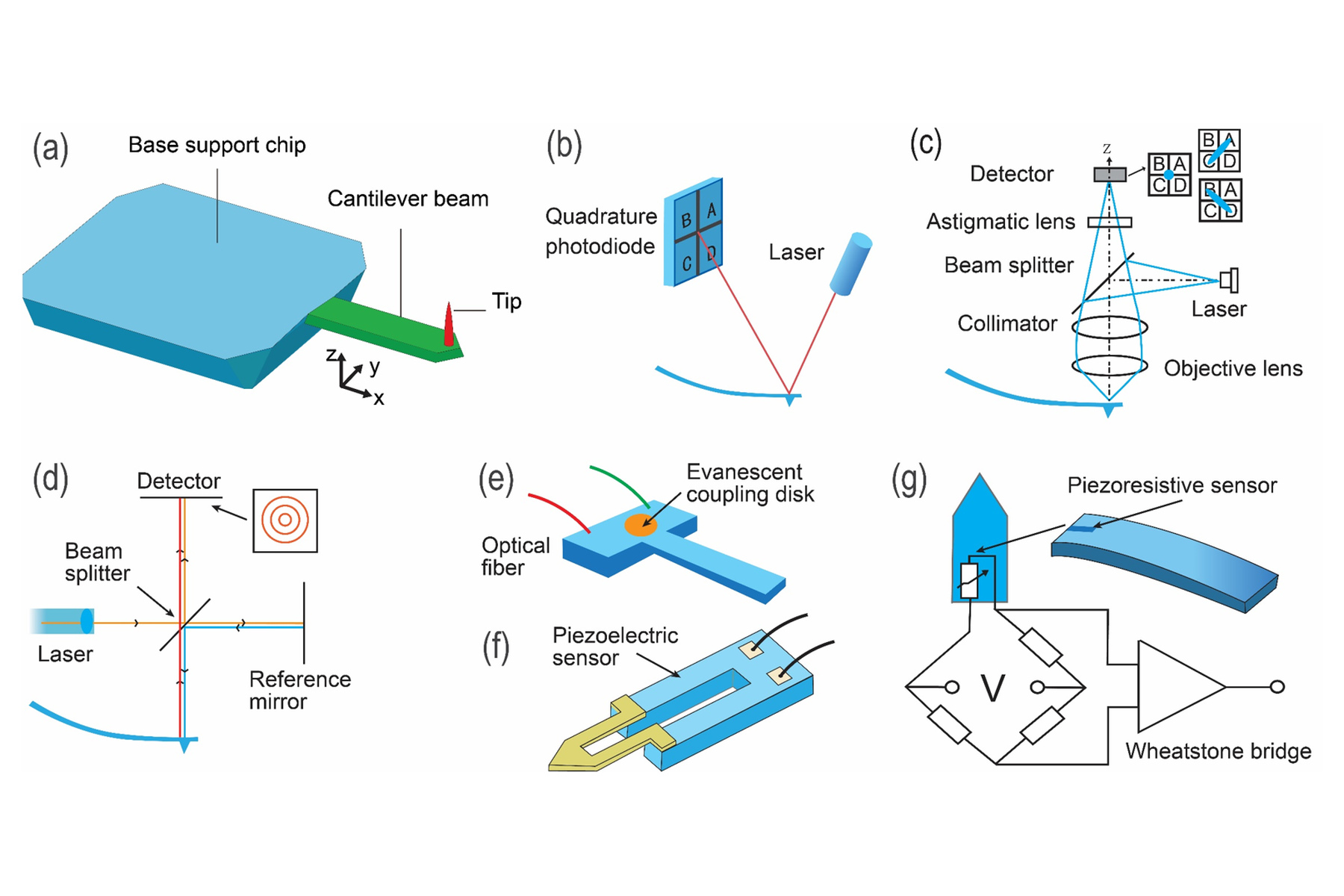
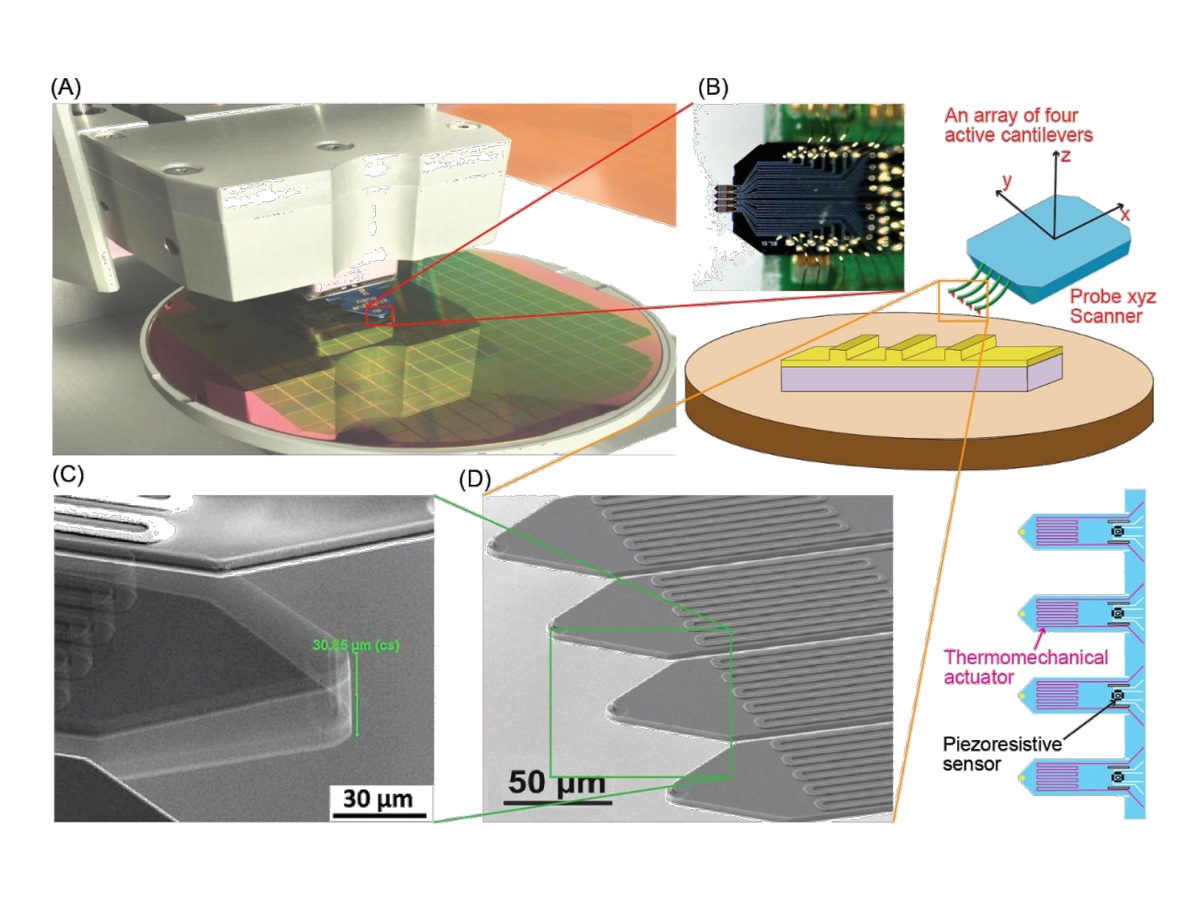
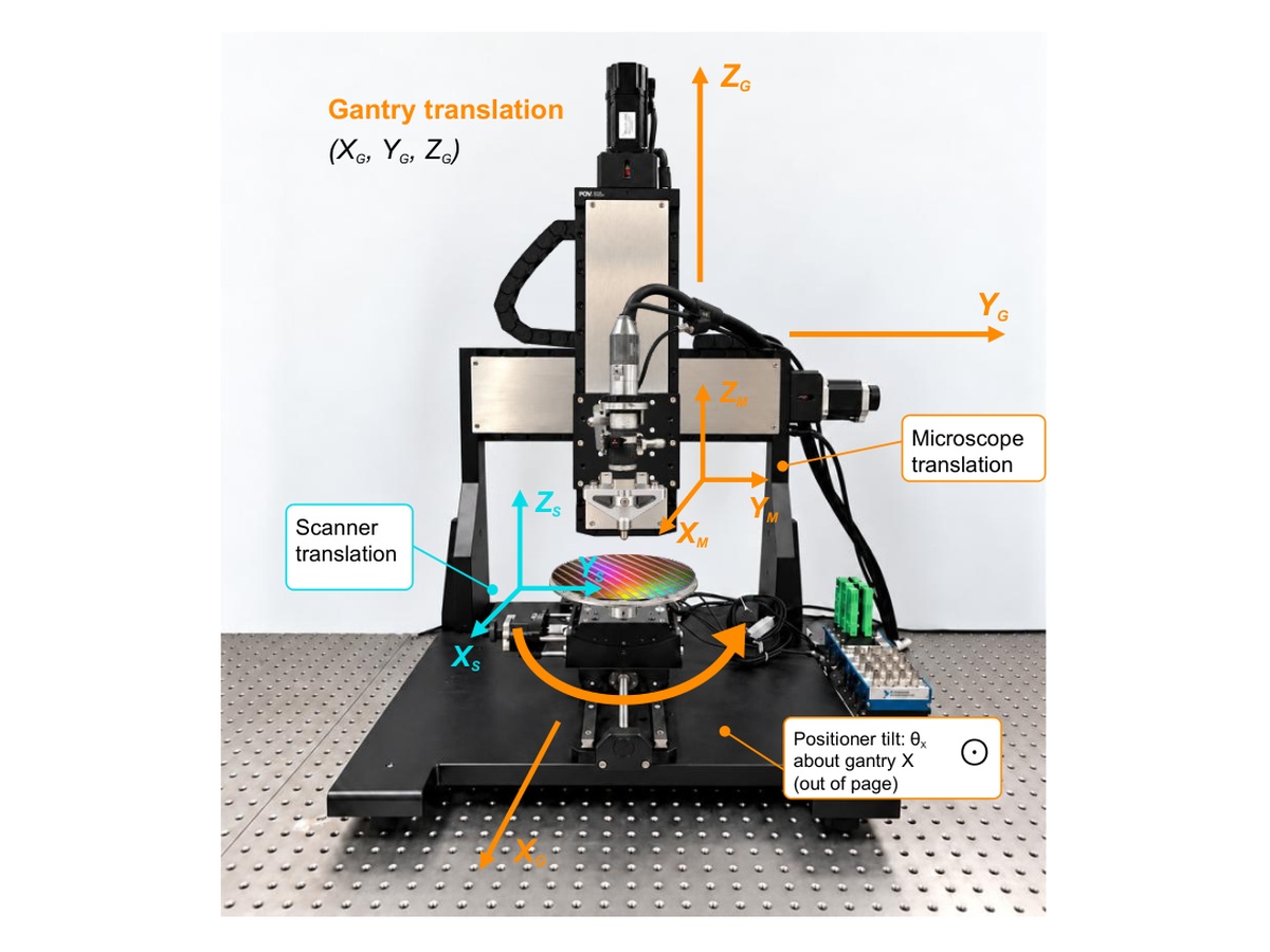
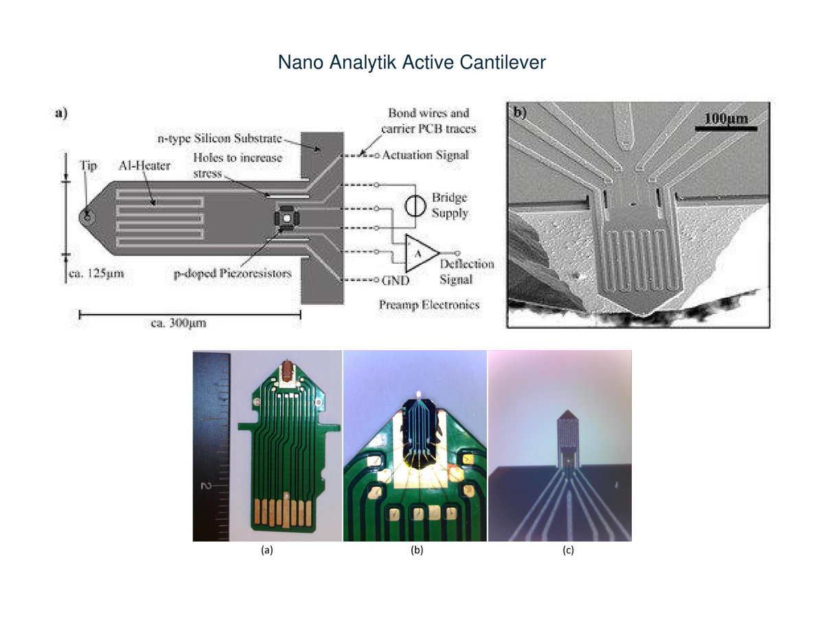
Miniaturized active cantilevers integrate actuation and sensing at the probe, providing a route to parallel wafer-scale measurement and complementary measurements in a single pass.

  • Objective: Develop custom active-probe arrays and the positioning, readout, and characterization tools needed for large-area, multimodal AFM.
  • Significance: Parallel probes expand the inspected area while on-probe actuation reduces dependence on the bandwidth of a shared scanner.
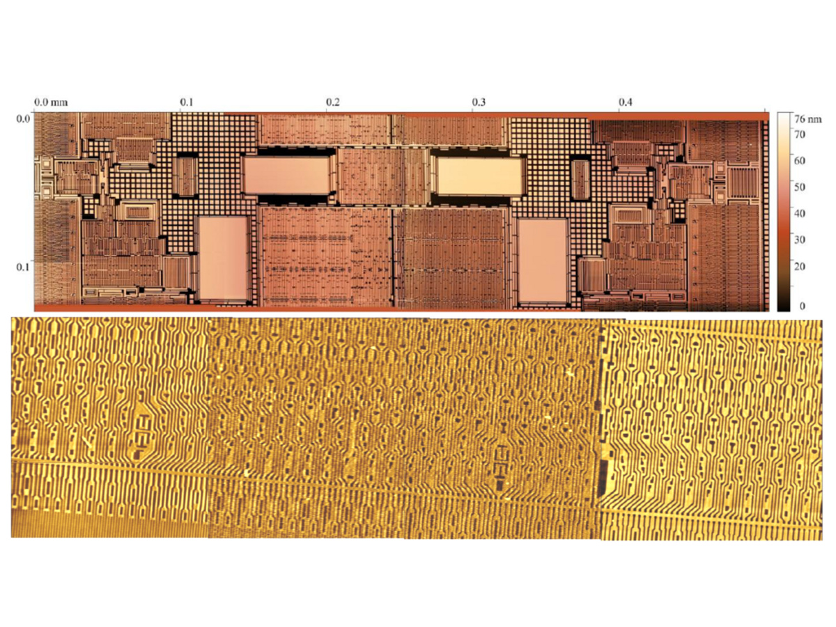
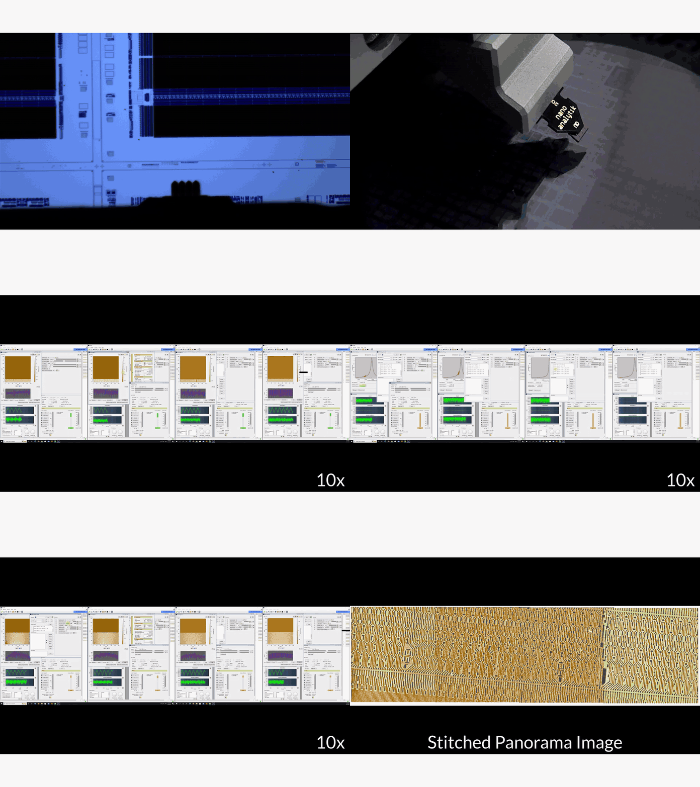
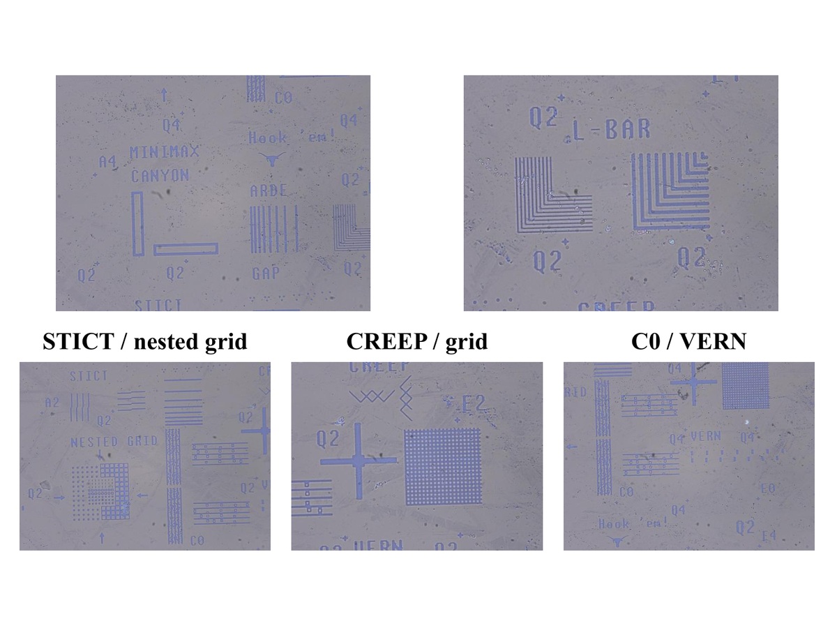
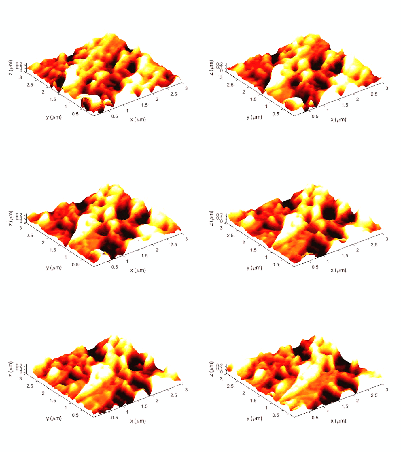
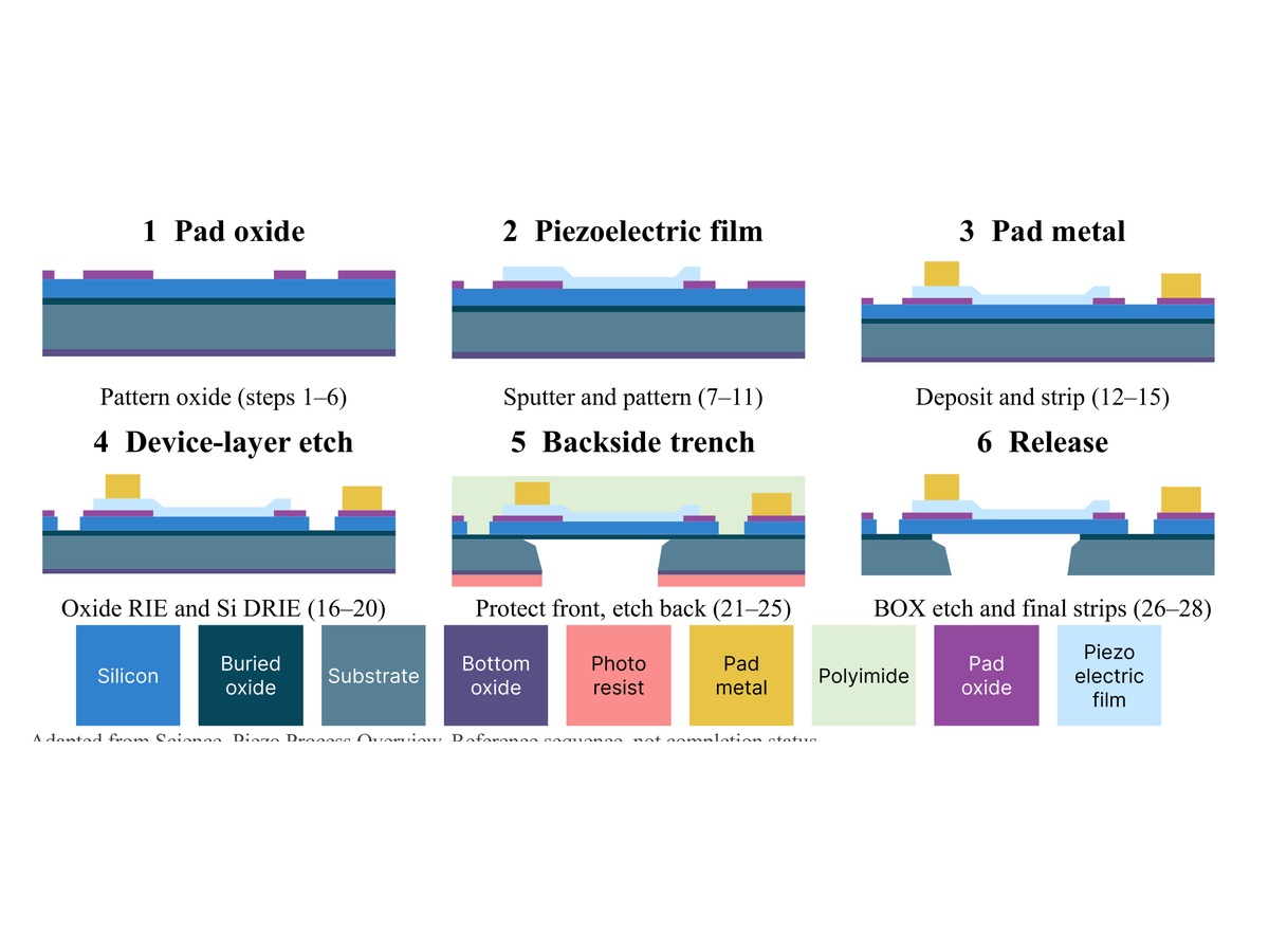
  • Result: Prior work demonstrated four-probe parallel inspection and a 500 µm × 125 µm EUV-mask panorama. Current UT work has established probe designs, on-campus fabrication steps, a gantry, and characterization hardware; multimodal imaging integration remains ongoing.

JoVE: Instrument Overview

JoVE: Wafer Imaging Demonstration

Published prior work: four active cantilevers for parallel wafer inspection, Journal of Visualized Experiments, 196, e65210 (2023).

Double-Probe Tilt Compensation and Imaging

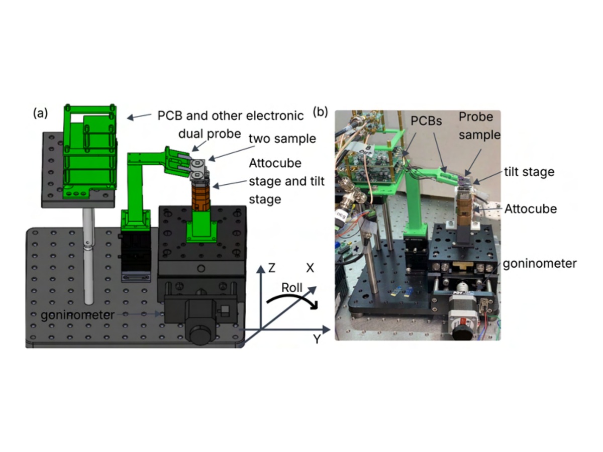
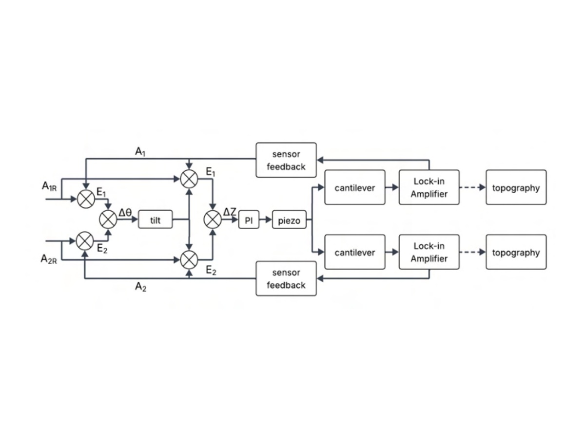
Parallel AFM needs more than additional probes: each probe must engage the surface while shared motion compensates for sample tilt. Our dual-probe testbed coordinates coarse angular alignment, fine tilt actuation and vertical positioning using the two cantilever amplitude signals.

  • Objective: Bring spatially separated active probes into stable engagement and maintain their amplitude setpoints during scanning.
  • Significance: Automatic tilt and height coordination addresses a practical obstacle to scaling AFM from one probe to parallel inspection.
  • Result: Demonstrated dual-probe engagement and amplitude regulation with coordinated tilt and height compensation.

Representative study: “Sample Tilt Control for Atomic Force Microscopes with Multiple Parallel Active Cantilevers,” 2026 American Control Conference.

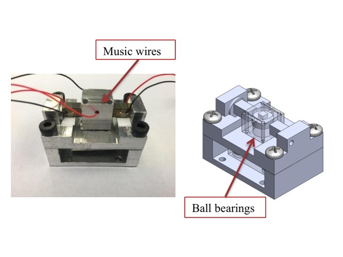
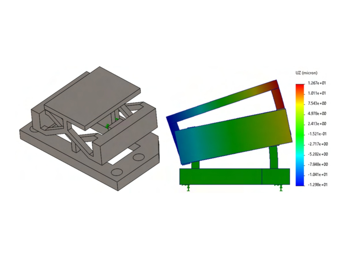
CAD model and assembled dual-probe AFM with coordinated height and tilt positioning.

Dual-Probe Tilt Testbed

CAD model and assembled dual-probe AFM with coordinated height and tilt positioning.

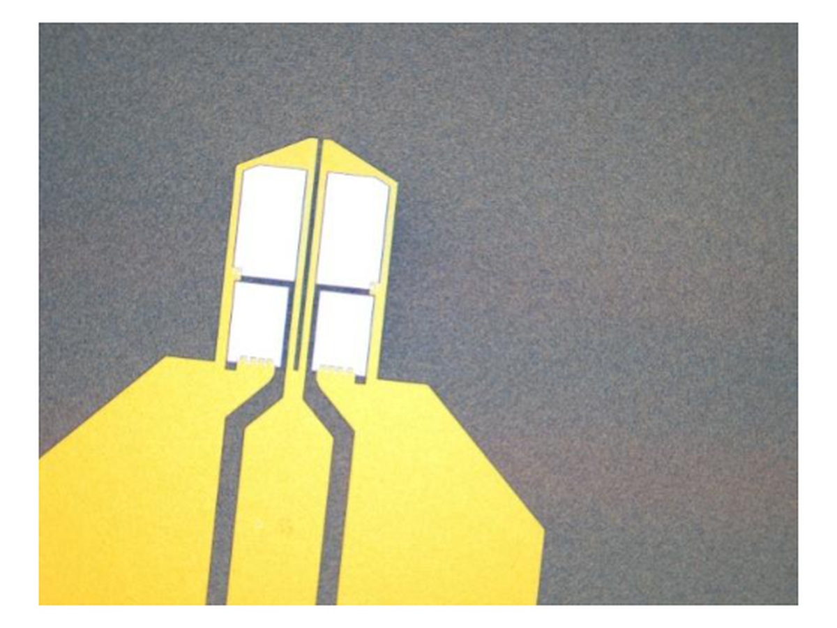
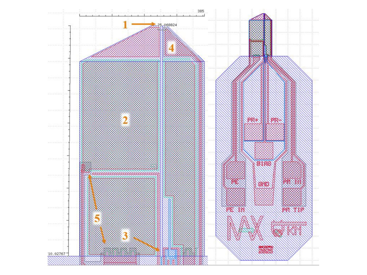
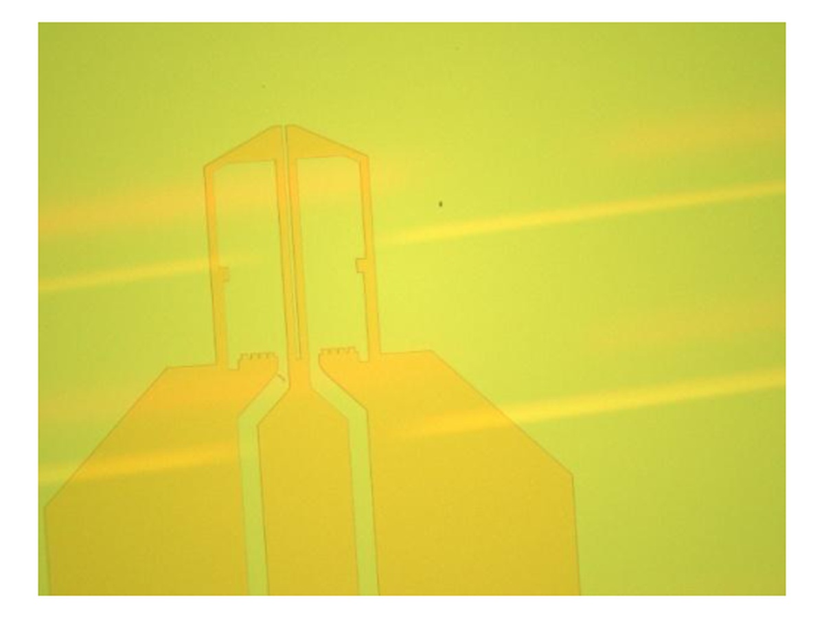
Microscope image after AlN etching in the active-probe fabrication process.

AlN Probe Fabrication

Microscope image after AlN etching in the active-probe fabrication process.

Dual-Probe Engagement

Amplitude records show engagement and regulation during dual-probe scanning.

Thermal Probe Nonlinearity

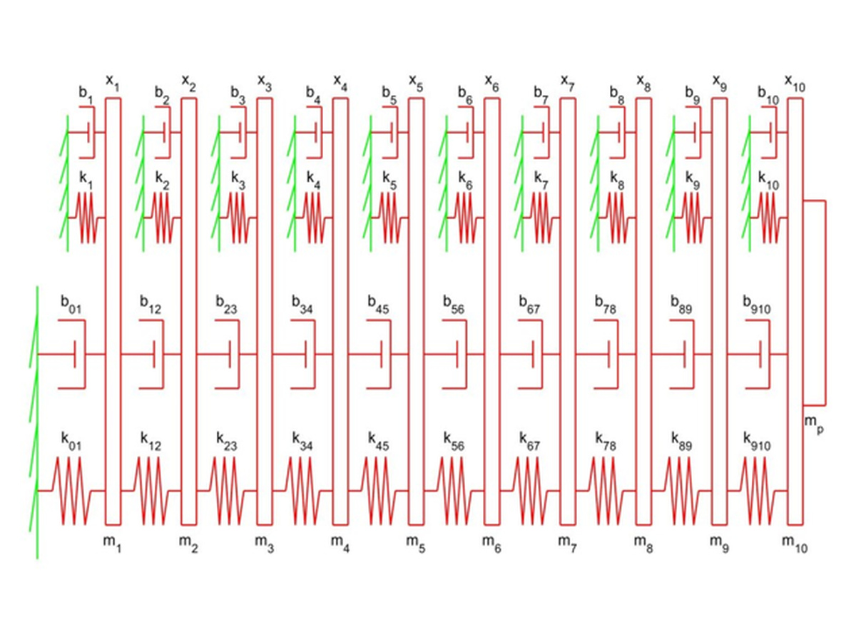
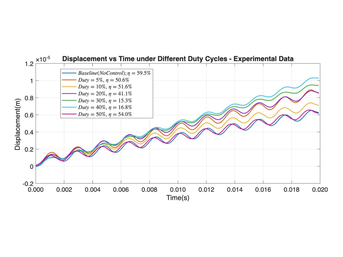
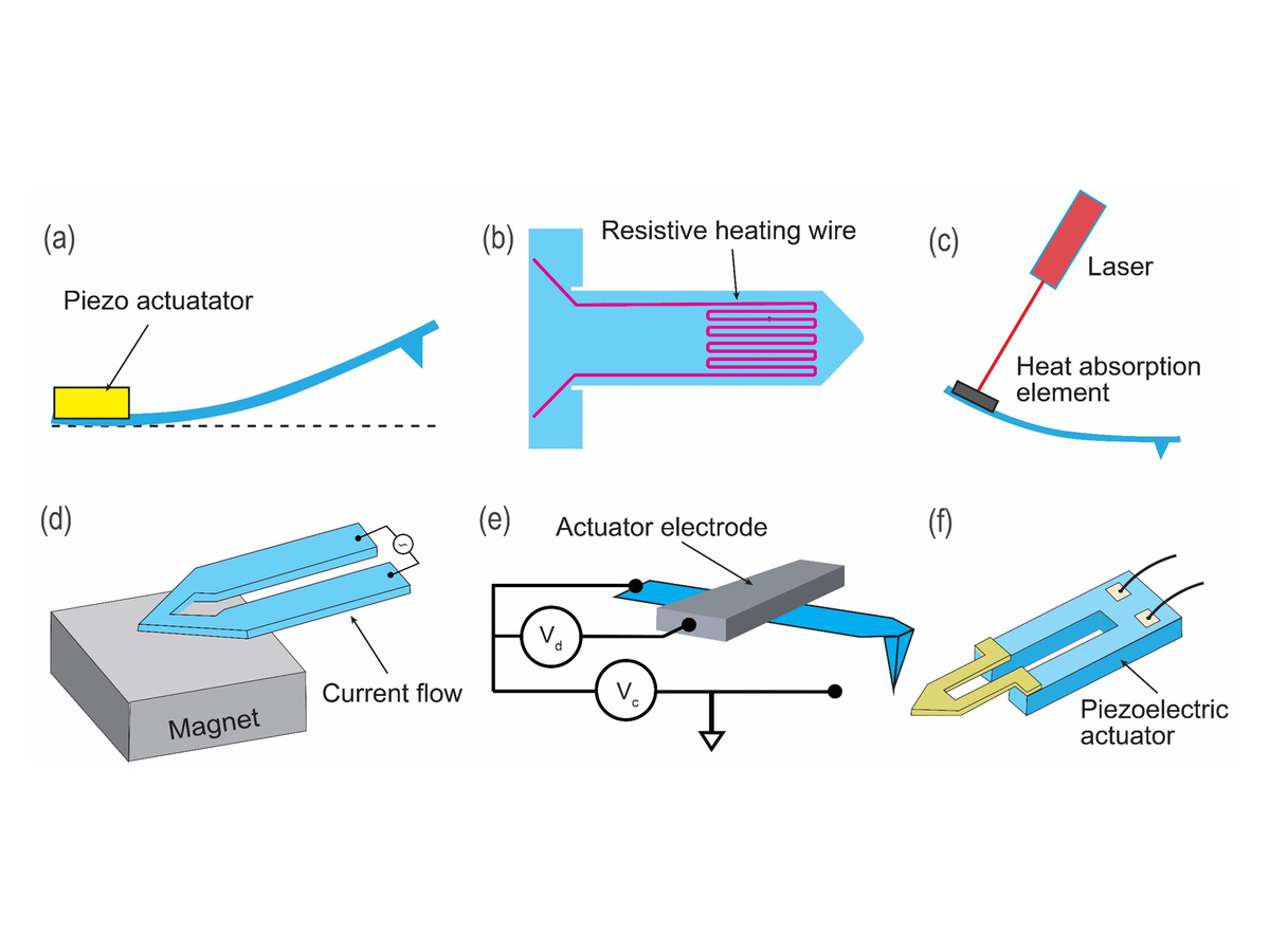
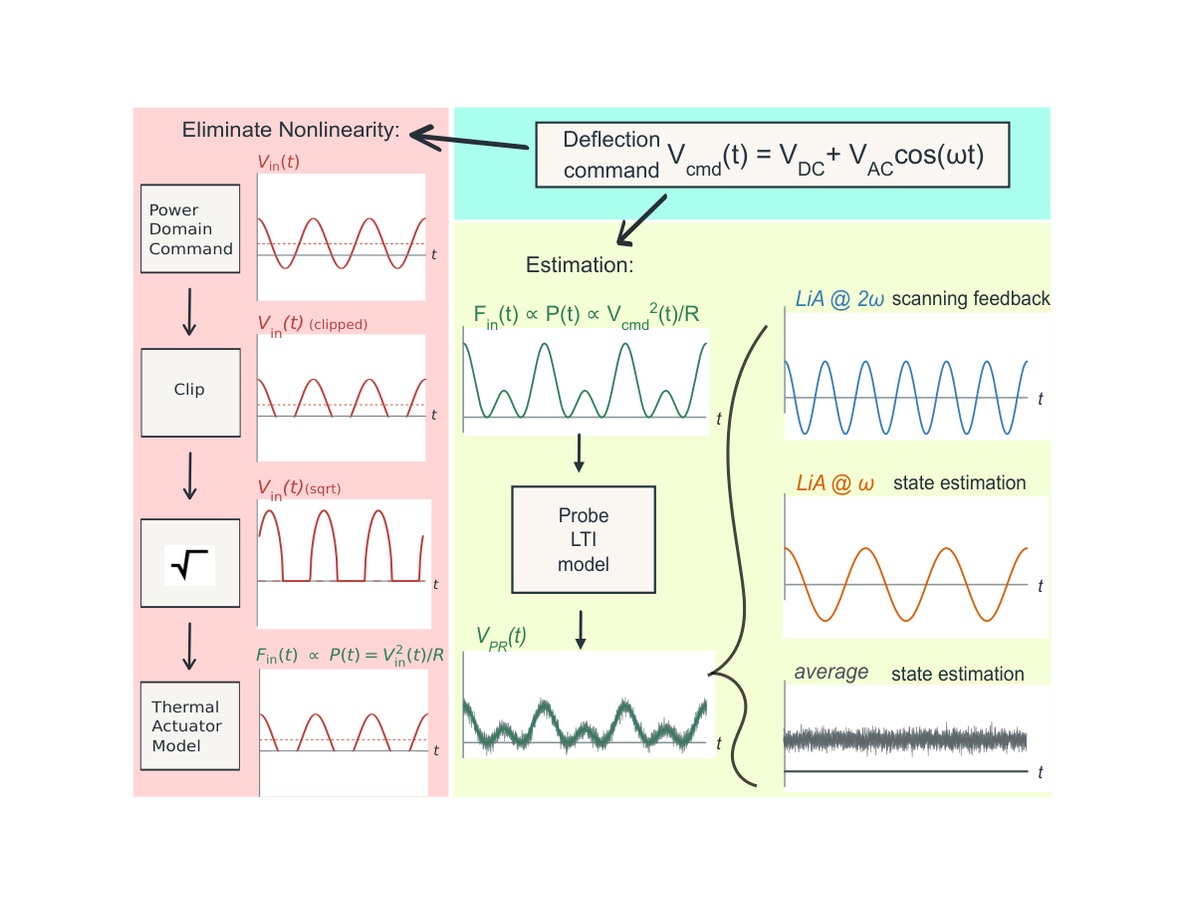
An electrothermal active cantilever uses the same heater for mean bending and oscillatory excitation. We characterize the resulting nonlinear coupling and implement power-domain compensation and probe feedback to control these motions more independently.

  • Objective: Compensate the quadratic voltage-to-power relation while regulating active-probe position and resonance behavior.
  • Significance: Predictable on-probe actuation supports compact, faster AFM and provides a building block for parallel-probe systems.
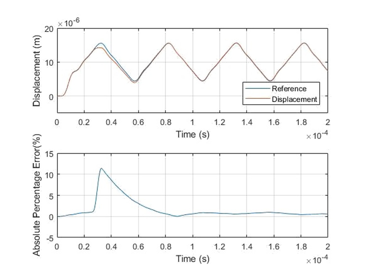
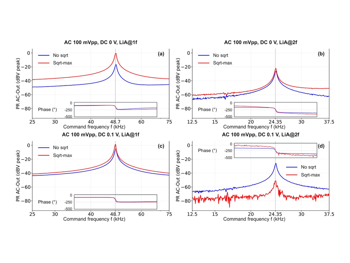
  • Result: Bench measurements show a 25.1 dB reduction in the sampled second-harmonic resonance peak at matched commands. Separate active-feedback tests reduce apparent Q from 423 to 235.
Probe construction and measured approximately quadratic command-to-bending response.

Electrothermal Probe Coupling

Probe construction and measured approximately quadratic command-to-bending response.

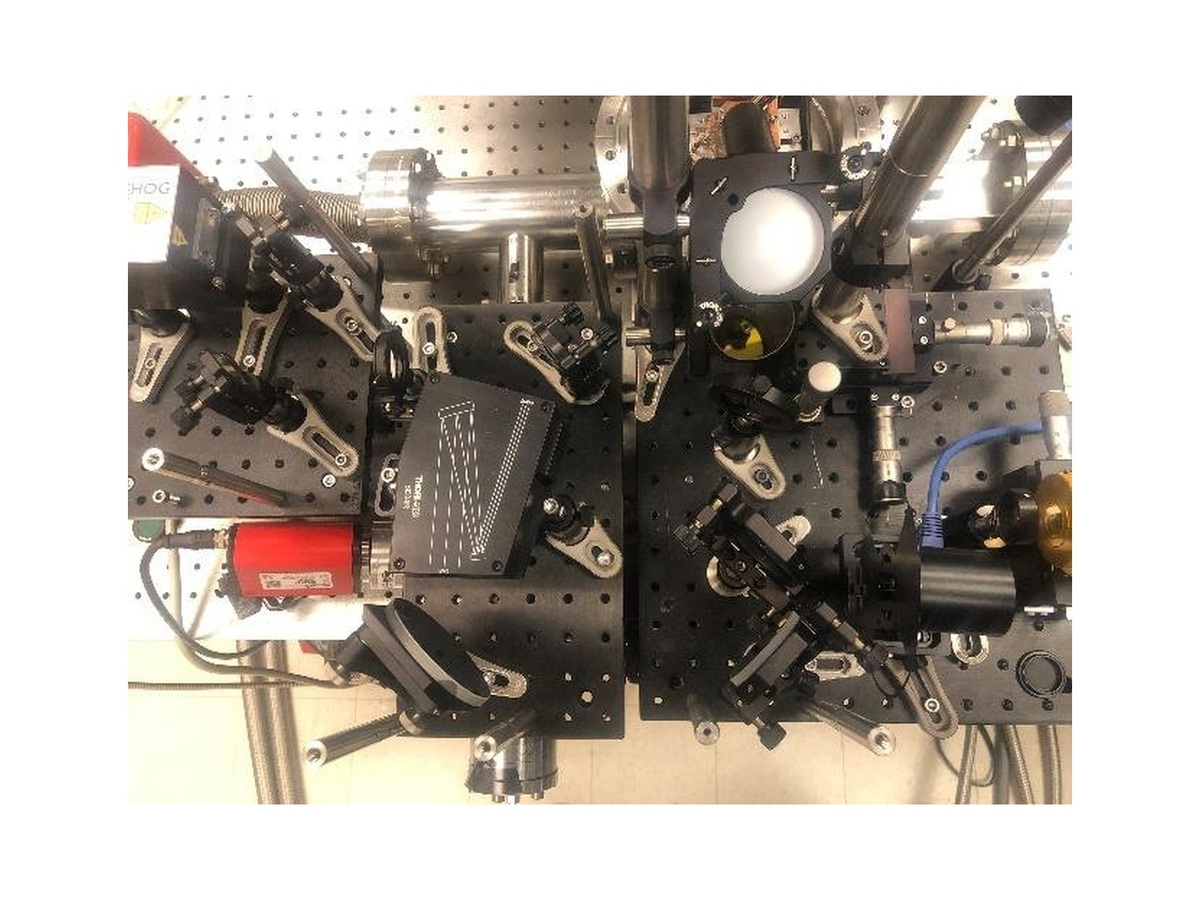
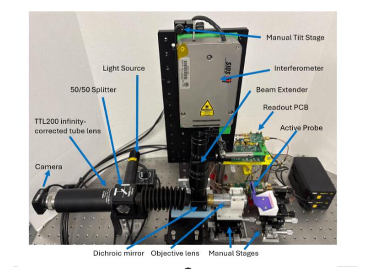
Interferometer, imaging optics and readout electronics characterize active-probe displacement.

Interferometric Characterization

Interferometer, imaging optics and readout electronics characterize active-probe displacement.

At matched command settings, compensation reduces the sampled second-harmonic resonance peak by 25.1 dB.

Measured Harmonic Attenuation

Compensation reduces the second-harmonic peak by 25.1 dB at matched commands.

Quantum Twisting Microscopy (QTM)

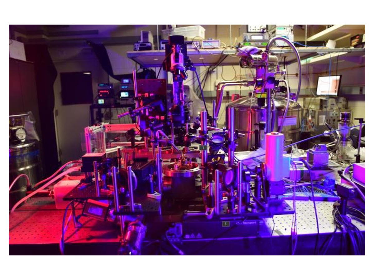
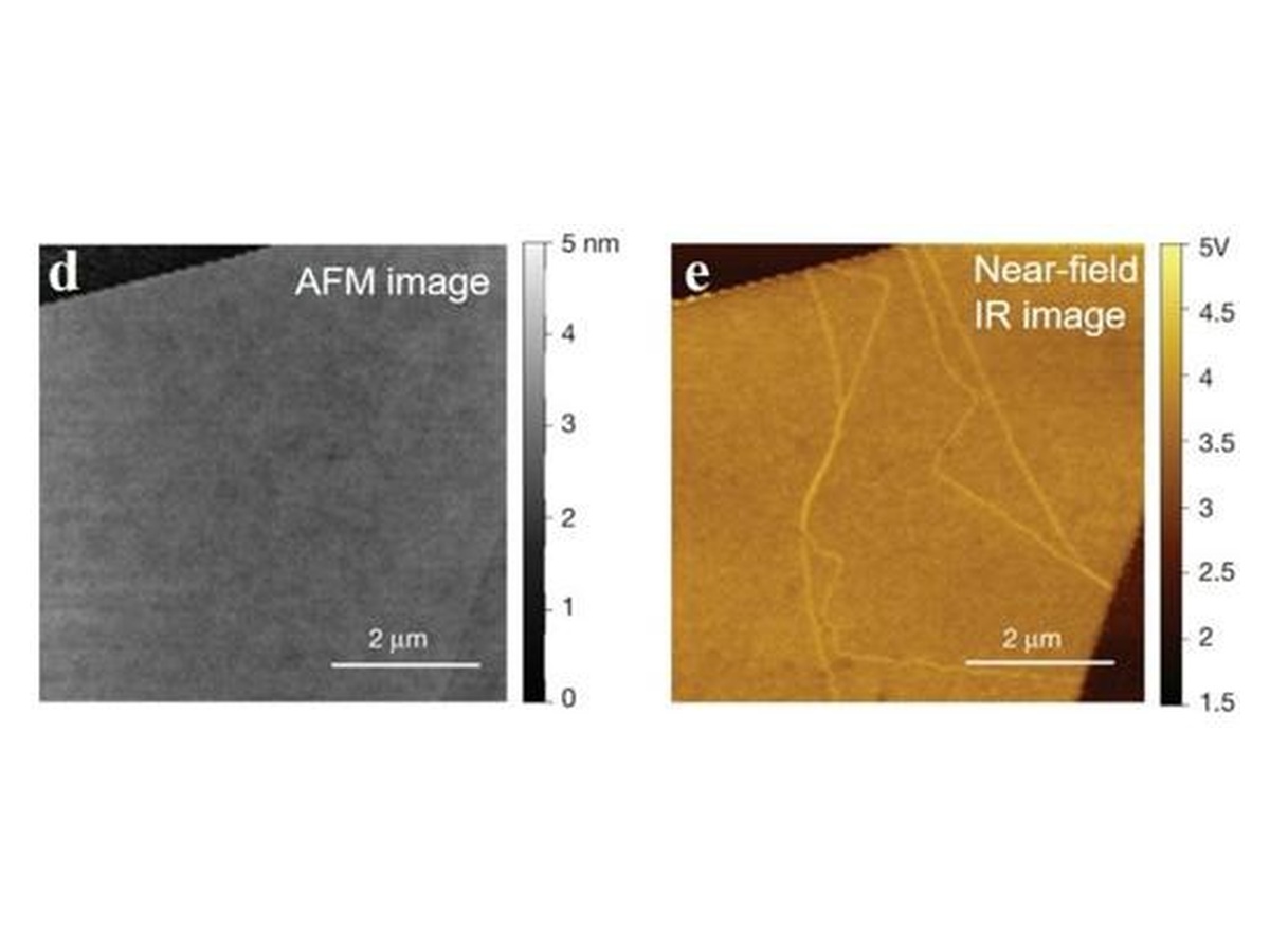
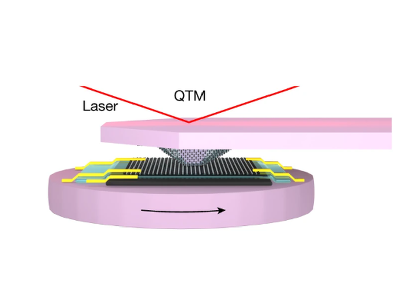
In collaboration with UT Austin physics researchers, we build precision probe and sample positioning systems for studying electronic coupling in two-dimensional materials as their relative twist angle changes.

  • Objective: Integrate independent probe and sample stages, rotation-center alignment, tilt compensation, and functionalized active probes.
  • Significance: A rotating tunnel junction reveals how twist angle affects interactions between two-dimensional layers.
  • Result: The mechanical platform and probe-functionalization workflow have been implemented, with microscopy-based alignment and ongoing work toward low-temperature probe characterization.
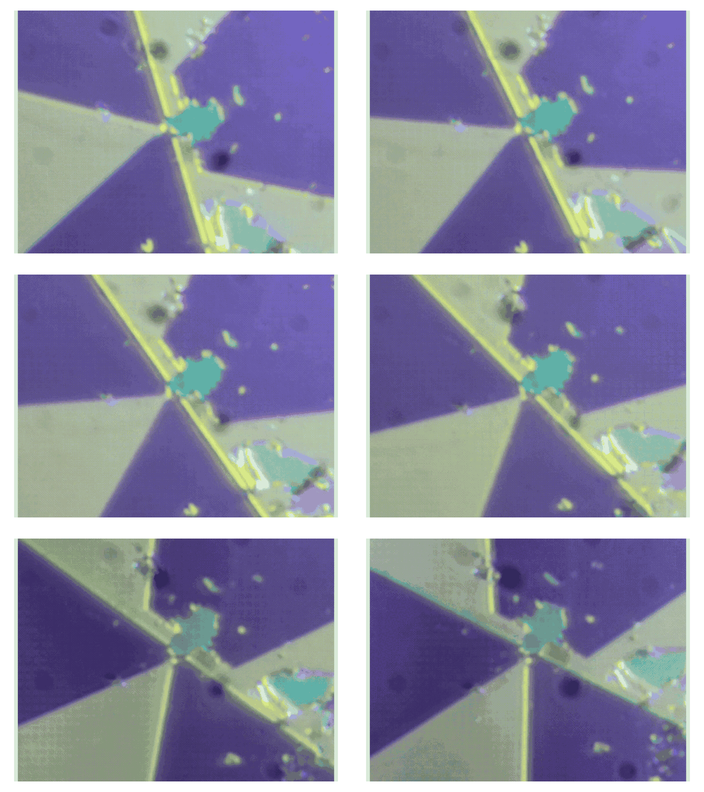
Animation of two overlaid atomic lattices showing how relative twist changes the moiré pattern.

Twistronics

Relative rotation of two-dimensional lattices changes the moiré pattern.

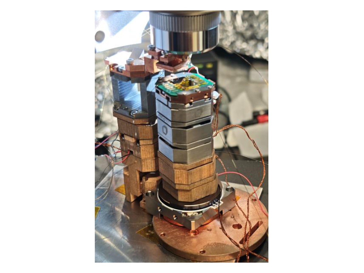
Implemented mechanical platform for quantum twisting microscopy.

QTM Instrument Platform

Implemented mechanical platform for quantum twisting microscopy.

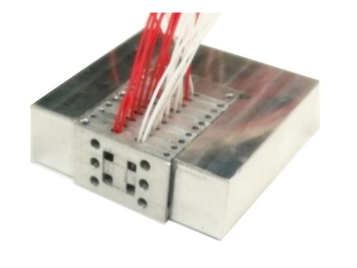
FIB-deposited pyramid on an active cantilever for 2D material transfer.

FIB Probe Functionalization

FIB-deposited pyramid on an active cantilever for 2D material transfer.

Sponsors and Collaborators

Sponsors: Samsung Electronics · Department of Energy · UT ME Startup Funds

Collaborators: Prof. Ken Shih · Prof. Leo Jia · Prof. Ivo Rangelow

Back to Research   |   Explore Advanced Mechatronics II

© MINIMAX Lab, Walker Department of Mechanical Engineering, The University of Texas at Austin. All rights reserved.